Powered By

Free XML Skins for Blogger

Powered by Blogger

Sunday, October 19, 2008

AC'97


AC'97

Short for Audio Codec, AC'97 is an Intel audio component that is integrated into Intel chipsets.

  • Users who are looking for AC'97 drivers or other onboard motherboard sound drivers should see document CH000660.


Codec

  1. Short for COmpression / DECompression, a codec is an algorithm or special computer program that reduces the number of bytes consumed by large files. Codecs are often used with videos distributed over the Internet; codecs enable what would normally be a very large video file to be much smaller. Users familiar with MP3 audio files can think of a Divx or XviD codec as the MP3 of videos.
  2. In communication, a codec is short for coder/decoder. A codec is a chip that decodes analog-to-digital conversion and digital-to-analog.

To resolve many issues related to a codec, users should download the latest codec from either the media player provider or from the developer of the type of video or audio file being played.

Microsoft Windows 2000 and XP users can easily view the audio and video codecs installed on their computer by opening the "Sound, video and game controllers" category in the Device Manager.

Where to get codecs:

One of our most recommended codec pack is the CCCP also known as the Combined Community Codec Pack you can find this download on their web page.

In addition to the above recommendation Free-Codecs.com has another great all in one codec package available under "Codec Pack All in 1".

Additional codecs available from Microsoft can also be found here.

Finally, a great list of hundreds of different codes can be found here.

  • Also see document CH000541 for additional information about why you may be able to hear a video but not see the video.
  • See document CH000682 for additional information to why you may be seeing the video but hearing no sound.

AGP

Accelerated Graphics Port

The Accelerated Graphics Port (also called Advanced Graphics Port, often shortened to AGP) is a high-speed point-to-point channel for attaching a graphics card to a computer's motherboard, primarily to assist in the acceleration of 3D computer graphics. Since 2004, AGP is being progressively phased out in favor of PCI Express. However, as of mid 2008 new AGP cards and motherboards are still available for purchase, though OEM driver support is minimal.

History

The AGP slot first appeared on x86 compatible system boards based on Socket 7 Pentium and Slot 1 Pentium II processors. Intel introduced AGP support with the i440LX Slot 1 chipset in mid-October 1997 and a flood of products followed from all the major system board vendors.

The first Socket 7 chipsets to support AGP were the VIA Apollo VP3, SiS 5591/5592, and the ALI Aladdin V. Intel never released an AGP-equipped Socket 7 chipset. FIC demonstrated the first Socket 7 AGP system board in November 1997 as the FIC PA-2012 based on the VIA Apollo VP3 chipset, followed very quickly by the EPoX P55-VP3 also based on the VIA VP3 chipset which was first to market.

Early video chipsets featuring AGP support included the Rendition Vérité V2200, 3dfx Voodoo Banshee, Nvidia RIVA 128, 3Dlabs PERMEDIA 2, Intel i740, ATI Rage series, Matrox Millennium II, and S3 ViRGE GX/2. Some early AGP boards used graphics processors built around PCI and were simply bridged to AGP. This resulted in the cards benefiting little from the new bus, with the only improvement used being the 66 MHz bus clock, with its resulting doubled bandwidth over PCI, and bus exclusivity. Examples of such cards were the Voodoo Banshee, Vérité V2200, Millennium II, and S3 ViRGE GX/2. Intel's i740 was explicitly designed to exploit the new AGP feature set. In fact it was designed to texture only from AGP memory, making PCI versions of the board difficult to implement (local board RAM had to emulate AGP memory.)

Microsoft first introduced AGP support into Windows 95 OEM Service Release 2 (OSR2 version 1111 or 950B) via the USB SUPPLEMENT to OSR2 patch. After applying the patch the Windows 95 system became Windows 95 version 4.00.950 B. The first Windows NT-based operating system to receive AGP support was Windows NT 4.0 with service pack 3, introduced in 1997. Linux support for AGP enhanced fast data transfers was first added in 1999 with the implementation of the AGPgart kernel module.

Versions of AGP

Intel released the first version of AGP; appropriately titled “AGP specification 1.0,” in 1997. It included both the 1x and 2x speeds. Specification 2.0 documented AGP 4X and 3.0 documented 8X. Available versions include:

AGP 1x
A 32-bit channel operating at 66 MHz resulting in a maximum data rate of 266 megabytes per second (MB/s), doubled from the 133 MB/s transfer rate of PCI bus 33 MHz / 32-bit; 3.3 V signaling.
AGP 2x
A 32-bit channel operating at 66 MHz double pumped to an effective 133 MHz resulting in a maximum data rate of 533 MB/s; signaling voltages the same as AGP 1x;
AGP 4x
A 32-bit channel operating at 66 MHz quad pumped to an effective 266 MHz resulting in a maximum data rate of 1066 MB/s (1 GB/s); 1.5 V signaling;
AGP 8x
A 32-bit channel operating at 66 MHz, strobing eight times per clock, delivering an effective 533 MHz resulting in a maximum data rate of 2133 MB/s (2 GB/s); 0.8 V signaling.

There are various physical interfaces (i.e. shape of slots), as explained in the Compatibility section below.

AGP version 3.5 is only publicly mentioned by Microsoft under Universal Accelerated Graphics Port (UAGP), which specifies mandatory supports of extra registers once marked optional under AGP 3.0. Upgraded registers include PCISTS, CAPPTR, NCAPID, AGPSTAT, AGPCMD, NISTAT, NICMD. New required registers include APBASELO, APBASEHI, AGPCTRL, APSIZE, NEPG, GARTLO, GARTHI.

Variations

A number of non-standard variations of the AGP interface have been produced by manufacturers.

64-bit AGP
A 64-bit channel. Used in high-end professional graphic cards. It was once proposed as an optional standard for AGP 3.0 in draft documents, but was dropped in the final version of the standard.
Ultra-AGP, Ultra-AGPII
It is an internal AGP interface standard used by SiS for the north bridge controllers with integrated graphics. The original version supports same bandwidth as AGP 8x, while Ultra-AGPII has maximum 3.2GB/s bandwidth.
AGP Pro
This was a rarely-used slot for cards that required more electrical power. It is a longer slot with additional pins for that purpose. AGP Pro cards were usually workstation-class cards used to accelerate professional computer-aided design applications employed in the fields of architecture, machining, engineering, simulations, and similar fields.

PCI-based AGP ports

AGP Express
Not a true AGP interface, but rather a way to allow an AGP card to be connected over the legacy PCI bus on a PCI Express motherboard. It is a technology found on ECS motherboards, and is used as a selling point for AGP card owners who want a new motherboard but do not want to be forced to buy a PCIe graphics card as well (most new motherboards do not provide AGP slots, only PCIe slots). An "AGP Express" slot is basically a PCI slot (with the electrical power of two) in the AGP form factor. While it offers backward compatibility with AGP cards, its disadvantages include incomplete support (some AGP cards do not work with AGP Express) and reduced performance - the card is forced to use the shared PCI bus at its lower bandwidth, rather than having exclusive use of the faster AGP.
AGI
The ASRock Graphics Interface (AGI) is a proprietary variant of the Accelerated Graphics Port (AGP) standard. Its purpose is to provide AGP-support for those of Asrock's motherboards that use chipsets lacking native AGP-support. However, it's not fully compatible and several videocard chipsets are known to not be supported.
AGX
The EpoX Advanced Graphics eXtended (AGX) is also a proprietary variant of the Accelerated Graphics Port (AGP) standard. It shares the same problems with the AGI port explained above. User manuals even recommend not using AGP 8X ATI cards with AGX slots.
XGP
The Biostar Xtreme Graphics Port is also a variant of the Accelerated Graphics Port (AGP) standard. It is similar to the two standards above, in that it supports AGP cards with chipsets that do not support AGP. Also like the above, it has support issues with many AGP cards.
AGR
The Advanced Graphics Riser is a variation of the AGP port used in some PCIe motherboards to offer a limited backwards compatibility with AGP. It is, effectively, a modified PCI slot with no direct interconnection with the CPU or memory, and thus slower even compared to an AGP 1x slot. Its actual compatibility with AGP cards is also limited, while motherboard manufacturers usually publish a specific compatibility list.

Compatibility


Compatibility, AGP Keys on card (top), on slot (bottom)

AGP cards are backward and forward compatible within limits. 1.5 V-only keyed cards will not go into 3.3 V slots and vice versa, though "Universal" slots exist which accept either type of card. AGP Pro cards will not fit into standard slots, but standard AGP cards will work in a Pro slot. Some cards, like Nvidia's GeForce 6 series or ATI's Radeon X800 series, only have keys for 1.5 V to prevent them from being installed in older mainboards without 1.5 V support. Some of the last modern cards with 3.3 V support were the Nvidia GeForce FX series and the ATI Radeon 9500/9700/9800(R350) (but not 9600/9800(R360)).

It is important to check voltage compatibility as some cards incorrectly have dual notches and some motherboards incorrectly have fully open slots. Furthermore, some poorly designed older 3.3 V cards incorrectly have the 1.5 V key. Inserting a card into a slot that does not support the correct signaling voltage may cause damage.

There are some proprietary exceptions to this rule. For example, Apple Power Macintosh computers with the Apple Display Connector (ADC) have an extra connector which delivers power to the attached display. Additionally, moving cards between computers of various CPU architectures may not work due to firmware issues.

Use today

As of 2008, few new motherboards feature AGP slots. No new motherboard chipsets are equipped with AGP support, but motherboards continue to be produced with older chipsets that have AGP support. PCI Express allows for higher data transfer rates, has more robust full-duplex support, and also supports other devices.

All new graphics processors are designed for PCI-Express. To create AGP graphics cards, those chips require an additional PCIe to AGP bridge chip to convert PCIe signals to and from AGP signals. This incurs additional board costs due to the need for the additional bridge chip and for a separate AGP-designed circuit board.

Various manufacturers of graphics cards continue to produce AGP cards for the shrinking AGP user-base. The first bridged cards were the GeForce 6600 and ATI Radeon X800 XL boards, released during 2004-5. As of late 2007, AGP cards from Nvidia are limited to the older GeForce 7 series boards. AMD's only official DirectX 10-capable AGP cards are from ATI's Radeon HD 2400 and 2600 budget and mid-range lines. As of April 2008 several manufacturers released AGP cards based on the mid-range Radeon HD3650 and the mid-high end HD3850.

AT keyboard

AT keyboard

Also known as the 101-key keyboard, the AT keyboard is the US standard keyboard introduced in 1986 by IBM and is used with the IBM compatible computer. This is one of the most common keyboards used today and can easily be identified as a keyboard that does not include the extra three Windows keys introduced by Microsoft. An AT keyboard may also be used to describe a keyboard that uses the AT (Din5) port; this type of keyboard has been widely replaced by new standards such as PS/2 and USB keyboards. Below is an example of the AT interface found on the back computers.

AT Bus

Used for the IBM AT and compatible computers to transfer information from one component to the other at speeds of up to 16-bits of data at a time.

ATX

ATX


The ATX (for Advanced Technology Extended) form factor was created by Intel in 1995. It was the first big change in computer case and motherboard design in many years. ATX overtook AT completely as the default form factor for new systems. ATX addressed many of the AT form factor's annoyances that had frustrated system builders. Other standards for smaller boards (including microATX, FlexATX and mini-ITX) usually keep the basic rear layout but reduce the size of the board and the number of expansion slot positions. In 2003, Intel announced the BTX standard, intended as a replacement for ATX. As of 2007 the ATX form factor remains the industry standard for do-it-yourselfers; BTX has however made inroads into pre-made systems, being adopted by computer makers like Dell, Gateway, and HP.

The official specifications were released by Intel in 1995, and have been revised numerous times since, the most recent being version 2.2, released in 2004.

A full size ATX board is 305mm wide by 244mm deep (12" x 9.6" ). This allows many ATX form factor chassis to accept microATX boards as well.

AT-style computer cases had a power button that was directly connected to the system computer power supply (PSU). The general configuration was a double-pole latching mains voltage switch with the four pins connected to wires from a four-core cable. The wires were either soldered to the power button (making it difficult to replace the power supply if it failed) or blade receptacles were used.

Typical ATX power supply

Typical ATX power supply
Interior view of an ATX power supply.

Interior view of an ATX power supply.

An ATX power supply does not directly connect to the system power button, allowing the computer to be turned off via software. However, many ATX power supplies have a manual switch on the back to ensure the computer is truly off and no power is being sent to the components. With this switch on, energy still flows to the components even when the computer appears to be "off." This is known as soft-off or standby and can be used for remote wake up through Wake-on-Ring or Wake-on-LAN, but is generally used to power on the computer through a front switch.

The power supply's connection to the motherboard was changed. Older AT power supplies had two similar connectors that could be accidentally switched, usually causing short-circuits and irreversible damage to the motherboard. ATX used one large, keyed connector instead, making a reversed connection very difficult. The new connector also provided a 3.3 volt source, removing the need for motherboards to derive this voltage from one of the other power rails. Some motherboards, particularly late model AT form factor offerings, supported both AT and ATX PSUs.

ATX was originally designed with the power supply drawing air into the case and exhausting it down onto the motherboard. The plan was to deliver cool air directly to the CPU's and power regulation circuitry's location, which was usually at the top of the motherboard in ATX designs. This was not particularly useful for a variety of reasons. Early ATX systems simply didn't have processors or components with thermal output that required special cooling considerations. Later ATX systems with significantly greater heat output would not be aided in cooling by a power supply delivering its often significantly heated exhaust into the case. As a result, the ATX specification was changed to make PSU airflow optional.

With the introduction of the Pentium 4, the standard 20-pin ATX power connector was deemed inadequate to supply increasing electrical load requirements. The standard was revised with an extra 4-pin, 12-volt connector. This was later adopted by Athlon XP and Athlon 64 systems. Various high-end systems may have other forms of supplemental power connections.

Because video card power demands have dramatically increased over the 2000s, some high-end graphics cards have power demands that exceed AGP or PCIe slot capabilities. For these cards, supplementary power was delivered through a standard power connector like those used for hard drives or floppy drives. PCI Express-based video cards manufactured after 2004 typically use a standard 6 or 8-pin PCIe power connector directly from the PSU.

Because the ATX PSU uses the motherboard's power switch, turning on the power in situations that do not utilize an ATX motherboard is possible by shorting the green wire from the ATX connector to any black wire on the connector (or ground). This allows re-use of an old PC power supply for tasks other than powering a PC, but one must be careful to observe the minimum load requirements of the PSU.

The ATX form factor has had five main power supply designs throughout its lifetime:

  • ATX — 20 pin connector (Used for all of pentium range)
  • WTX — 24 pin connector (Xeon and Athlon MP)
  • AMD GES — 24 pin main connector, 8 pin secondary connector (some dual-processor Athlon)
  • EPS12V — 24 pin main connector, 8 pin secondary connector, optional 4 pin tertiary connector (Xeon and Opteron) defined in SSI specification
  • ATX12V — 20 pin main connector, 4 pin secondary connector, 8 pin tertiary connector (Pentium 4 and mid/late Athlon XP & Athlon 64)
    • ATX12V 1.3 — guidance for the −5 volt feed was removed. This was only used by legacy ISA add-in cards.
    • ATX12V 2.0 — 20 pin main connector, 4 pin secondary connector (Pentium 4, Core 2 Duo, and Athlon 64 with PCI Express)
    • ATX12V 2.1 — One 20-pin connector, one ATX12V 4 pin connector. Many power supply manufacturers include a 4 plus 4 pin, or 8 to 4 pin secondary connector instead, which can also be used as the secondary EPS12V connector.
    • ATX12V 2.2 — One 24-pin connector, one ATX12V 4 pin connector. Main Power Connector changed from 20 pin to 24 pin to support PCI-Express requirements.
24-pin ATX power supply connector
(20-pin omits the last 4: 11, 12, 23 and 24)
Color Signal Pin Pin Signal Color

+3.3 V 1 13 +3.3 V sense

+3.3 V 2 14 −12 V

Ground 3 15 Ground

+5 V 4 16 Power on

Ground 5 17 Ground

+5 V 6 18 Ground

Ground 7 19 Ground

Power good 8 20 −5 V (optional)

+5 V standby 9 21 +5 V

+12 V 10 22 +5 V

+12 V 11 23 +5 V

+3.3 V 12 24 Ground

Dell power supplies

Older Dell computers, particularly those from the Pentium II and III times, are notable for using proprietary power wiring on their power supplies and motherboards. While the motherboard connectors appear to be standard ATX, and will actually fit a standard power supply, they are not compatible. Not only have wires been switched from one location to another, but the number of wires for a given voltage has been changed. Thus, the pins cannot simply be rearranged.

The change affects not only 20-pin ATX connectors, but also auxiliary 6-pin connectors. Modern Dell systems may use standard ATX connectors.Dell PC owners should be careful when attempting to mix non-Dell motherboards and power supplies, as it can cause damage to the power supply or other components. If the power supply color coding on the wiring does not match ATX standards, then it is probably proprietary. Wiring diagrams for Dell systems are usually available on Dell's support page.

Connectors

ATX I/O plates

ATX I/O plates

On the back of the system, some major changes were made. The AT standard had only a keyboard connector and expansion slots for add-on card backplates. Any other onboard interfaces (such as serial and parallel ports) had to be connected via flying leads to connectors which were mounted either on spaces provided by the case or brackets placed in unused expansion slot positions. ATX allowed each motherboard manufacturer to put these ports in a rectangular area on the back of the system, with an arrangement they could define themselves (though a number of general patterns depending on what ports the motherboard offers have been followed by most manufacturers). Generally the case comes with a snap out panel, also known as an I/O plate, reflecting one of the common arrangements. If necessary, I/O plates can be replaced to suit the arrangement on the motherboard that is being fitted and the I/O plates are usually included when purchasing a motherboard. Panels were also made that allowed fitting an AT motherboard in an ATX case.

ATX also made the PS/2-style mini-DIN keyboard and mouse connectors ubiquitous. AT systems used a 5 pin DIN connector for the keyboard, and were generally used with serial port mice (although PS/2 mouse ports were also found on some systems). Many modern motherboards are phasing out the PS/2-style keyboard and mouse connectors in favor of the modern standard of USB ports. Other legacy connectors that appeared on ATX motherboards but are being phased out include 25-pin parallel ports and 9-pin RS-232 serial ports. In their place, on-board Ethernet, Firewire, eSATA and audio ports are increasingly common.


BAT

BABY AT

Baby AT motherboard.

Baby AT motherboard.

In 1985 IBM introduced Baby AT. Soon after all computer makers abandoned AT for the cheaper and smaller Baby AT, using it for computers from the 286 processors to the first Pentiums. These motherboards have similar mounting hole positions and the same eight card slot locations as those with the AT form factor, but are 2" (51 mm) narrower and marginally shorter. The size (220x330 mm) and flexibility of this kind of motherboard were the key to success of this format. While now obsolete, a few computers are still using it, and modern PC cases are generally backwards compatible to fit Baby AT.

In 1995, Intel introduced ATX, a form factor which gradually replaced older Baby AT motherboards. During the late 1990s, a great majority of boards were either Baby AT or ATX. Many motherboard manufacturers continued making Baby AT over ATX since many computer cases and power supplies in the industry were still compatible with AT boards and not ATX boards. Also, the lack of an eighth slot on ATX motherboards kept it from being used in some servers. After the industry adapted to ATX specifications, it became common to design cases and power supplies to support both Baby AT and ATX motherboards.

BTX

BTX (form factor)


BTX (for Balanced Technology Extended) is a form factor for PC motherboards, originally slated to be the replacement for the aging ATX motherboard form factor in late 2004 and early 2005. It has been designed to alleviate some of the issues that arose from using newer technologies (which often demand more power and create more heat) on motherboards compliant with the circa-1996 ATX specification. The ATX and BTX standards were both proposed by Intel. Intel's decision to refocus on low-power CPUs, after suffering scaling and thermal issues with the Pentium 4, has added some doubt to the future of the form factor. The first company to implement BTX was Gateway Inc, followed by Dell. Apple's Mac Pro utilizes the elements of the BTX design system as well but is not BTX compliant. However, future development of BTX retail products by Intel was canceled in September 2006.


Enhancements

  • Low-profile - With the push for ever-smaller systems, a redesigned backplane that shaves inches off height requirements is a benefit to system integrators and enterprises who use rack mounts or blade servers.
  • Thermal design - The BTX layout establishes a straighter path of airflow with fewer obstacles, resulting in better overall cooling capabilities. A distinct feature of BTX is the vertical mounting of the motherboard on the left-hand side. This results in the graphics card heatsink or fan facing upwards, rather than in the direction of the adjacent expansion card.
  • Structural design - The BTX standard specifies different locations for hardware mounting points, thereby reducing latency between devices and also reduces the physical strain imposed on the motherboard by heat sinks, capacitors and other components dealing with electrical and thermal regulation. For example, the Northbridge and Southbridge chips are located near each other and to the hardware they control.

Pico BTX

BTX form factor motherboard inside a Dell Dimension E520.

BTX form factor motherboard inside a Dell Dimension E520.

Pico BTX is a computer motherboard and system form factor. Pico BTX motherboards are relatively small—smaller than current 'micro'-sized motherboards, hence the name 'pico'. They share a common top half with the other sizes in the BTX line, but sport only one or two expansion slots, designed for half-height or riser-card applications.

Intel, as the originator of the form factor, is the primary manufacturer of such boards. As of January 2007, there are very limited numbers of OEM motherboards and cases for Pico BTX. Complete systems are available from Dell, which embraced BTX quickly within its desktop product line, and appears to use Pico BTX boards in its smallest machines, though no claims are made by Dell in their marketing materials.

Compatibility with ATX products

The BTX form factor motherboards are incompatible with the ATX form factor cases and vise versa. The areas where incompatibility doesn't apply is in power supplies, parallel hardware, processors, RAM, hard drives, and ROM devices.

Chipset


Chipset


  1. A designated group of microchips that are designed to work with one or more related functions that were first introduced in 1987. When referring the the main motherboard chipset such as the Intel Chipsets, these chipsets will generally include the functions of the CPU, PCI, ISA, USB, etc... An example of an Intel chipset is the i820 or the Intel 820 chipset
  1. Chips or Chips and Technologies is also a computer company. See our chips company information page for additional information about this company.
Diagram of a motherboard chipset


Communication and Network Riser

Communications and Networking Riser

Communications and Networking Riser, or CNR, is a slot found on certain PC motherboards and used for specialized networking, audio, and telephony equipment. A motherboard manufacturer can choose to provide audio, networking, or modem functionality in any combination on a CNR card. CNR slots were once commonly found on Pentium 4-class motherboards, but have since been phased out in favor of on-board or embedded components.

Technology

Physically, a CNR slot has two rows of 30 pins, with two possible pin configurations: Type A and Type B, each with different pin assignments. CNR Type A uses 8-pin network interface, while Type B uses 16-pin Media Independent Interface (MII) bus LAN interface. Both types carry USB and AC'97 signals.

As with AMR, CNR had the cost savings potential for manufacturers by removing analog I/O components from the motherboard. This allowed the manufacturer to only certify with the FCC for the CNR card, and not the entire motherboard. This resulted in a quicker production-to-market time for new motherboards, and allowed mass-production of CNR cards to be used on multiple motherboards.

The ACR slot was a competing specification developed by a group of third-party vendors. Its principal advantage over CNR was the backwards-compatible slot layout which allowed it to use both AMR and ACR cards. The same group also developed a physically smaller version, the MDC.

History

Modem for CNR slot.

Modem for CNR slot.

Intel developed the CNR slot to replace its own Audio/modem riser (AMR) technology, drawing on two distinct advantages over the AMR slot it replaced; CNR was both capable of being either software based (CPU-controlled) or hardware accelerated (dedicated ASIC), and was plug-and-play compatible. On some motherboards, a CNR slot replaced the last PCI slot, but most motherboard manufacturers engineered boards which allow the CNR and last PCI slot to share the same space.

As of 2007, with the integration of components such as Ethernet and audio into the motherboard, the CNR is obsolete, and is not found on the most recent full sized motherboards. It can still be found on smaller form-factor motherboards (like microATX) with lower end processors, where it continues to perform its original function.

Tuesday, October 14, 2008

CMOS

CMOS

Complementary metal–oxide–semiconductor (CMOS) (pronounced "see-moss", IPA: /siːmɔːs, ˈsiːmɒs/), is a major class of integrated circuits. CMOS technology is used in microprocessors, microcontrollers, static RAM, and other digital logic circuits. CMOS technology is also used for a wide variety of analog circuits such as image sensors, data converters, and highly integrated transceivers for many types of communication. Frank Wanlass successfully patented CMOS in 1967 (US Patent 3,356,858).

CMOS was also sometimes referred to as complementary-symmetry metal–oxide–semiconductor (or COS-MOS). The words "complementary-symmetry" refer to the fact that the typical digital design style with CMOS uses complementary and symmetrical pairs of p-type and n-type metal oxide semiconductor field effect transistors (MOSFETs) for logic functions.

Two important characteristics of CMOS devices are high noise immunity and low static power consumption. Significant power is only drawn when the transistors in the CMOS device are switching between on and off states. Consequently, CMOS devices do not produce as much waste heat as other forms of logic, for example transistor-transistor logic (TTL) or NMOS logic, which uses all n-channel devices without p-channel devices. CMOS also allows a high density of logic functions on a chip.

Technical Details

"CMOS" refers to both a particular style of digital circuitry design, and the family of processes used to implement that circuitry on integrated circuits (chips). CMOS circuitry dissipates less power when static, and is denser than other implementations having the same functionality. As this advantage has grown and become more important, CMOS processes and variants have come to dominate, so that the vast majority of modern integrated circuit manufacturing is on CMOS processes.

CMOS circuits use a combination of p-type and n-type metal–oxide–semiconductor field-effect transistors (MOSFETs) to implement logic gates and other digital circuits found in computers, telecommunications equipment, and signal processing equipment. Although CMOS logic can be implemented with discrete devices (for instance, in an introductory circuits class), typical commercial CMOS products are integrated circuits composed of millions (or hundreds of millions) of transistors of both types on a rectangular piece of silicon of between 0.1 and 4 square centimeters.[citation needed] These devices are commonly called "chips", although within the industry they are also referred to as "die" (singular) or "dice", "dies", or "die" (plural).

Composition

The main principle behind CMOS circuits that allows them to implement logic gates is the use of p-type and n-type metal–oxide–semiconductor field-effect transistors to create paths to the output from either the voltage source or ground. When a path to output is created from the voltage source, the circuit is said to be pulled up. On the other hand, the circuit is said to be pulled down when a path to output is created from ground.

Inversion


Static CMOS Inverter

CMOS circuits are constructed so that all PMOS transistors must have either an input from the voltage source or from another PMOS transistor. Similarly, all NMOS transistors must have either an input from ground or from another NMOS transistor. The composition of a PMOS transistor creates low resistance when a low voltage is applied to it and high resistance when a high voltage is applied to it. On the other hand, the composition of an NMOS transistor creates high resistance when a low voltage is applied to it and low resistance when a high voltage is applied to it.

The image on the right shows what happens when an input is connected to both a PMOS transistor and an NMOS transistor. When the voltage of input A is low, the NMOS transistor has high resistance so it stops voltage from leaking into ground, while the PMOS transistor has low resistance so it allows the voltage source to transfer voltage through the PMOS transistor to the output. The output would therefore register a high voltage.

On the other hand, when the voltage of input A is high, the PMOS transistor would have high resistance so it would block voltage source from the output, while the NMOS transistor would have low resistance allowing the output to drain to ground. This would result in the output registering a low voltage. In short, the outputs of the PMOS and NMOS transistors are complementary such that when the input is low, the output would be high, and when the input is high, the output would be low. Because of this, the CMOS circuits' output is by default the inversion of the input.

Duality

An important characteristic of a CMOS circuit is the duality that exists between its PMOS transistors and NMOS transistors. A CMOS circuit is created so that a path would always exist from the output to either the power source or ground. In order to accomplish this, the set of all paths to the voltage source must be the complement of the set of all paths to ground. This can be easily accomplished by defining one in terms of the NOT of the other. The logic works out through De Morgan's laws such that the PMOS transistors in parallel have corresponding NMOS transistors in series while the PMOS transistors in series have corresponding NMOS transistors in parallel.

Logic

NAND gate in CMOS logic

NAND gate in CMOS logic

More complex logic functions such as those involving AND and OR gates require manipulating the paths between gates to represent the logic. When a path consists of two transistors in series, then both transistors must have low resistance for voltage to pass, modeling an AND. When a path consists of two transistors in parallel, then either one or both of the transistors must have low resistance for voltage to pass, modeling an OR.

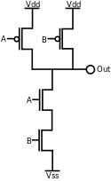
Shown on the right is a circuit diagram of a NAND gate in CMOS logic. If both of the A and B inputs are high, then both the NMOS transistors (bottom half of the diagram) will conduct, neither of the PMOS transistors (top half) will conduct, and a conductive path will be established between the output and Vss (ground), bringing the output low. If either of the A or B inputs is low, one of the NMOS transistors will not conduct, one of the PMOS transistors will, and a conductive path will be established between the output and Vdd (voltage source), bringing the output high.

An advantage of CMOS over NMOS is that both low-to-high and high-to-low output transitions are fast since the pull-up transistors have low resistance when switched on, unlike the load resistors in NMOS logic. In addition, the output signal swings the full voltage between the low and high rails. This strong, more nearly symmetric response also makes CMOS more resistant to noise.


Example: NAND gate in physical layout

The physical layout of a NAND circuit

The physical layout of a NAND circuit

This example shows a NAND logic device drawn as a physical representation as it would be manufactured. The physical layout perspective is a "bird's eye view" of a stack of layers. The circuit is constructed on a P-type substrate. The polysilicon, diffusion, and n-well are referred to as "base layers" and are actually inserted into trenches of the P-type substrate. The contacts penetrate an insulating layer between the base layers and the first layer of metal (metal1) making a connection.

The inputs to the NAND (illustrated in green coloring) are in polysilicon. The CMOS transistors (devices) are formed by the intersection of the polysilicon and diffusion: N diffusion for the N device; P diffusion for the P device (illustrated in salmon and yellow coloring respectively). The output ("out") is connected together in metal (illustrated in cyan coloring). Connections between metal and polysilicon or diffusion are made through contacts (illustrated as black squares). The physical layout example matches the NAND logic circuit given in the previous example.

The N device is manufactured on a P-type substrate. The P devices is manufactured in an N-type well (n-well). A P-type substrate "tap" is connected to VSS and an N-type n-well tap is connected to VDD to prevent latchup.

Power: switching and leakage

CMOS logic dissipates less power than NMOS logic circuits because CMOS dissipates power only when switching (dynamic power). On a typical ASIC in a modern 90 nanometer process, switching the output might take 120 picoseconds, and happen once every ten nanoseconds. NMOS logic dissipates power whenever the output is low (static power), because there is a current path from Vdd to Vss through the load resistor and the n-type network.

CMOS circuits dissipate power by charging the various load capacitances (mostly gate and wire capacitance, but also drain and some source capacitances) whenever they are switched. The charge moved is the capacitance multiplied by the voltage change. Multiply by the switching frequency on the load capacitances to get the current used, and multiply by voltage again to get the characteristic switching power dissipated by a CMOS device: P = CV2f.

A different form of power consumption became noticeable in the 1990s as wires on chip became narrower and the long wires became more resistive. CMOS gates at the end of those resistive wires see slow input transitions. During the middle of these transitions, both the NMOS and PMOS networks are partially conductive, and current flows directly from Vdd to Vss. The power thus used is called crowbar power. Careful design which avoids weakly driven long skinny wires has ameliorated this effect, and crowbar power is nearly always substantially smaller than switching power.

Both NMOS and PMOS transistors have a threshold gate-to-source voltage, below which the current through the device drops exponentially. Historically, CMOS designs operated at supply voltages much larger than their threshold voltages (Vdd might have been 5 V, and Vth for both NMOS and PMOS might have been 700 mV). But as supply voltages have come down to conserve power the Vdd to Vss short circuit is avoided.

However, to speed up the designs, manufacturers have switched to gate materials which lead to lower voltage thresholds and a modern NMOS transistor with a Vth of 200 mV has a significant subthreshold leakage current. Designs (e.g. desktop processors) which try to optimize their fabrication processes for minimum power dissipation during operation have been lowering Vth so that leakage power begins to approximate switching power. As a result, these devices dissipate considerable power even when not switching. Leakage power reduction using new material and system design is critical to sustaining scaling of CMOS. The industry is contemplating the introduction of High-k Dielectrics to combat the increasing gate leakage current by replacing the silicon dioxide that are the conventional gate dielectrics with materials having a higher dielectric constant. A good overview of leakage and reduction methods are explained in the book Leakage in Nanometer CMOS Technologies ISBN 0-387-25737-3.

Analog CMOS

Besides digital applications, CMOS technology is also used for analog applications. For example, there are CMOS operational amplifier ICs available in the market. CMOS technology is also widely used for RF applications all the way to microwave frequencies. Indeed, CMOS technology is used for mixed-signal (analog+digital) applications.

Temperature range

Conventional CMOS devices work over a range of -55 °C to +125 °C. There are indications that silicon CMOS will work down to 40 kelvins.

Controller

A device that controls the transfer of data from a computer to a peripheral device and vice versa. For example, disk drives, display screens, keyboards, and printers all require controllers.

In personal computers, the controllers are often single chips. When you purchase a computer, it comes with all the necessary controllers for standard components, such as the display screen, keyboard, and disk drives. If you attach additional devices, however, you may need to insert new controllers that come on expansion boards.

Controllers must be designed to communicate with the computer's expansion bus. There are three standard bus architectures for PCs -- the AT bus, PCI (Peripheral Component Interconnect), and SCSI. When you purchase a controller, therefore, you must ensure that it conforms to the bus architecture that your computer uses.

DB Connector

DB Connector

A type of connector that usually would hook to the parallel or serial port. Most common data base connectors are the DB-9, DB-15, DB-19, DB-25, DB-37, and DB-50, the number indicates how many active lines the connector has, but not always meaning how many pins.

DB-9 & DB-15

Additional information and help with the DB-9 and DB-15 or the standard PC serial port can be found on our serial port help page.

The DB-9 and DB-15 are also found on Network cards. The DB-9 cable is sometimes used for Token-Ring adapters and the DB-15 is used for the Thicknet coaxial cables. Additional information and help with network adapters can be found on our network help page.

The DB-9 port is also found on the NeXT computer used to connect laser printers.

DB-19

The DB-19 is a connector found on the Apple Macintosh, NeXT and some Atari computers, and is generally used to connect external disk drives.

DB-25

The DB-25 interface was an older type of serial connector. Additional information and help with serial ports can be found on our serial port help page.

The DB-25 port is also a type of SCSI interface. Additional information and help with SCSI can be found on our SCSI help page.

DB-37

Connector found on various network devices used to connect network hubs and other network devices and perform various other functions. Companies that utilize this cable include Cisco, Nortel, SMC...

The DB-37 connector is also used on other devices that connect such devices as sensors, switches, satellite antennas, control systems, video and audio studio automation, security control systems and various other equipment.

DB-50

SCSI connector that is rarely used or found today. Additional information and help with SCSI can be found on our SCSI help page.

Dual BIOS

Dual BIOS

A computer motherboard that contains two BIOS chips, a main BIOS and a backup BIOS. This type of motherboard setup helps a motherboard recover from any issues that may happen during a BIOS update, helps protect the BIOS from any potential virus, and helps with any other issues that may arise related to the BIOS.

Dual-BIOS Architecture


System Layout

Below is the firmware layout for our systems.

NAND Writer                      |--> NOR Flash
u-boot                          -
Linux kernel |--> NAND Flash
Rescue root filesystems -
Root Filesystems                 |--> CF or Hard Disk

The firmware (u-boot, Linux kernel and rescue root file system) is stored in NAND flash. Roof filesystem is stored in CF card or hard disk. In usual cases, the NAND flash itself cannot be used as a booting media. The NAND boot design of Samsung processor makes it possible to use NAND solely as a booting media. Under proper hardware configuration, the processor will automatically copy the first page of NAND flash to SDRAM and execute the boot code. (u-boot) The boot code is transferred into 4-kbytes steppingstone during reset. After the transfer, the boot code will be executed on the steppingstone. The NAND boot design will save the PCB space and product cost. However, since the bootloader and kernel are stored in the same NAND flash. The bootloader might be erased during software development or firmware upgrade by typing the wrong download address. In this case, people usually use ICE (In Circuit Emulation) to recover the bootloader. But using ICE is a tedious way and not convenient for software engineers or maintenance engineers. It is therefore; Embedian adopts a dual-BIOS design by adding a 0.5MB NOR flash and uses jumper selection to switch back to NOR boot when the u-boot in NAND flash been erased. A "NAND Writer" program in NOR could recover the system by setting the jumper to NOR boot. The default jumper setting is NAND boot.

Figure 1 shows the block diagram of NOR boot and NAND boot.

Figure 1. NOR boot and NAND boot

Below the "device" stands for the APC series single board computers or EBC series box computers.

1.2.1. NOR Boot

This section describes how to transfer and write u-boot image to NAND flash using NOR boot configuration. This is usual the case when the u-boot in NAND flash been erased. If you simply upgrade the firmware, you could use u-boot to upgrade u-boot itself without setting the jumper to NOR boot unless your u-boot in NAND is gone. The manufacturer's defualt is with NAND image and developers could design theirs own application directly and stored in CF or harddisk. Unless necessary, we don't recommend user alert the firmware in NAND.

1.2.1.1. Transfer and Write U-Boot Image to NAND Flash

To transfer and write u-boot image to NAND, first, power off device and set the jumper JP2 to NOR flash configuration. (Be sure to power off the system before you changing the jumper.) Install the USB host driver and DNW programs Embedian provided in your host Windows PC. Connect the serial console cable (10-1151-0809) from serial console port (CN6) of device to the COM port of your Windows PC. And connect a USB cable from USB device port (CN5) to USB host port of your Windows PC.

Open the DNW program in your Windows PC, in "Configuration", set the COM port as the following setting of figure 2. And the Download Address is "0x3000000", this is the SDRAM address where the program will be executed.

Figure 2. COM and USB Port Setting of DNW program

Power on device, and you should see the following screen in your DNW programs as shown in figure 3.

Figure 3. NOR Boot Download

Here the program will detect if the USB cable is connected, if not, the program will tell you to connect the USB cable. Plug the USB cable and USB is waiting for download the u-boot binary.

In "USB Port" of DNW program, click "Transmit" as following figure 4.

Figure 4. Configure USB Port

A file browser will ask you to transmit the file. Find the file "2440test.bin" in your PC and click. You will see the following screen.

Figure 5. NOR Boot Test Menu

Select the function "25: NAND Program" and press "Enter". You will see the following screen.

Figure 6. NAND Writer Menu

Select "9: K9F5608 Program" and press "Enter".

Now the "NAND Writer" program is ready to download u-boot to SDRAM of the device from your PC. You need to specify the download address as following instruction. In "Configuration" of DNW program, set the Download Address to "0x30100000" as following figure 6. This will download the program to SDRAM.

Figure 7. USB Download Address Setting for U-Boot

A file browser will ask you to transmit the file. Find the file "u-boot.bin" in your PC and click. The version of u-boot binary is build from original 1.1.4. u-boot source tree with some modification.

Now you are ready to write the u-boot to NAND flash from SDRAM. At "Input target block number:", type "0" and the u-boot will be written to NAND flash. This is to tell device writing u-boot to NAND flash from the 0th block. Figure 8 illustrates the above steps.

Figure 8. U-Boot Target Block

After the u-boot been written to NAND flash, set the jumper 2 back to NAND boot. And you will see u-boot menu in DNW (or you could use Hyper Terminal) program from the console.

1.2.2. NAND Boot

After you installed, upgraded or recovered the u-boot in NAND flash and running on your system, you can use the u-boot command line to download another u-boot image to replace the current u-boot, kernel image and rescue root file systems to boot Linux kernel without setting jumper JP2 back again unless your u-boot or writting address is typing wrong by accident. The NOR and NAND boot are completely hardware independent, and it is impossible to breach the data in NOR flash when you set to NAND boot. You could also use Linux kernel to download u-boot. We will detail the instructions in section 1.4.

Warning: Before you can install the new image, you have to erase the current one. If anything goes wrong your system will be dead. Set the jumper to NOR boot to rescue the system. It is strongly recommended that:

  • you have a backup of the old, working u-boot image. (You could also download from Embedian's website.)
  • you know how to install an image on a virgin system.
  • always power off the system before change the jumpers

Figure 9. U-Boot Screen

You can interrupt the "Count-Down" of autoboot and enter the command line interface of u-boot by pressing any key. If you have programmed a kernel and root filesystem into on-board flash using the procedures outlined in section 1.4, u-boot's environment variables will be set to automatically boot that system after the five-second delay. If u-boot is not interrupted by activity on the debug port, Linux will boot automatically and you will not receive a u-boot command prompt.

If you wish to alter the default behavior of u-boot, you should use the setenv command to change the environment variables. Once you have set the environment variables the way you want them, use the saveenv command to store your current environment into flash.

Two different command interpreters are available.

  • Simple command line interface
  • Bourne comaptible shell (HUSH shell from Busybox)
Configuration parameters and commands sequences (scripts !) can be stored in "environment variables" which can be saved to NAND flash storage. The next section will introduce the u-boot command line interface.

Wednesday, October 8, 2008

Extensible Firmware Interface


Extensible Firmware Interface
The Extensibile Firmware Interface specification defines a model for the interface between operating systems and platform firmware. The interface consists of data tables that contain platform-related information and boot and runtime service calls that are available to the operating system and its loader. Together, these provide a standard environment for booting an operating system and running pre-boot programs. Microsoft supports Extensibile Firmware Interface as the only firmware interface to boot Windows XP. Because the 64-bit version of Windows will not boot with BIOS or with System Abstraction Layer (SAL) alone, Extensibile Firmware Interface is a requirement for all Intel Itanium-based systems to boot Windows.

The IA-64 architecture defines the following three firmware layers:
Processor Abstraction Layer
System Abstraction Layer
Extensibile Firmware Interface
The Processor Abstraction Layer, System Abstraction Layer and Extensibile Firmware Interface layers work together to provide processor and system initialization for an operating system boot. Processor Abstraction Layer and System Abstraction Layer provide machine check abort handling and other processor and system functions which would vary from implementation to implementation.

The System Abstraction Layer is a firmware layer that isolates the operating system and other higher-level software from implementation differences in the platform, while the Processor Abstraction Layer is the firmware layer that abstracts the processor implementation.

ENHANCED IDE

Enhanced IDE

Enhanced IDE, also called EIDE, is a term that Western Digital coined in 1994 to represent a particular set of extensions it devised to the original AT Attachment standard. At that time, the official ATA standard was rather limiting, and work was progressing towards the new ATA-2 standard. Western Digital decided that it did not want to wait for the new standard, and also that it could better position itself as a market leader by creating a new feature set for (then) future drives. The name "Enhanced IDE" was presumably selected to build upon the common name for ATA then in popular use: IDE.

The original Enhanced IDE program included the following improvements over ATA:

  • ATA-2 Enhancements: EIDE includes all (most?) of the improvements that are defined as part of the ATA-2 standard, including the higher-speed transfer modes.
  • ATAPI: The EIDE definition includes support for non-hard-disk ATAPI devices on the IDE/ATA channel. Note that at that time, ATAPI was not part of the ATA standard at all.
  • Dual IDE/ATA Host Adapters: The EIDE standard specifically includes support for dual IDE/ATA channels, allowing four IDE/ATA/ATAPI devices to be used. (In fact, the ATA standard at the time never precluded the use of two IDE/ATA channels; it just was not commonly done.)

EIDE has become a widely-accepted term in the industry, which would be great if not for the fact that it is so incredibly confusing. Objections to EIDE include the following issues:

  • Proprietary Standard: EIDE is not an official standard, and it competed with other non-standard IDE/ATA terms like Fast ATA. Of course, that criticism applies not just to EIDE.
  • Scope: Much of the criticism of the original EIDE program is that its scope was too wide, and that it encompassed features that are really the domain of the BIOS. For example, support for dual IDE/ATA host adapters, meaning a secondary IDE/ATA channel, has nothing to do with the interface or the hard disk itself. And ATAPI is a standard that is defined for use with optical drives and other non-hard-disk devices, which again requires BIOS and driver support and really has nothing to do with the hard disk. At the time, other hard disk manufacturers not only excluded these from their own standard proposals (such as Fast ATA), they made a point of criticizing Western Digital for bringing these issues into the interface discussion.
  • The Word "Enhanced": The choice of the word "enhanced" was unfortunate, as it led to confusion in another area. At around the same time that EIDE was introduced, the 504 MB hard disk size barrier became a big issue. To work around this required an "enhanced BIOS". Because of the fact that both of these phrases use the word "enhanced", and because EIDE defines BIOS support standards, many people have come to think of the terms as interchangeable when they really are not. This has lead to claims that you need an enhanced IDE interface to support disks over 504 MB, when you don't--you just need an enhanced BIOS. As if this weren't bad enough, some companies advertised add-in cards with enhanced BIOSes as "enhanced IDE cards"! :^)
  • Redefinition: Since EIDE is Western Digital's term, they have the right to change its meaning, and unfortunately, they do this on a regular basis. At first, EIDE included only PIO modes up to mode 3; then mode 4 was added. When the new Ultra DMA modes came out, WD of course added support for them to their newest models, but they kept calling the drives "EIDE"! Today other drive manufacturers also say things like "EIDE compatible", leaving you wondering what exactly this means.

Some people in the hard disk industry apparently feel that the creation of "Enhanced IDE" was one of the worst things to ever happen to the IDE/ATA interface! I think that is probably a bit over-stated, though I do agree that it is probably one of the most confusing things to ever happen to the IDE/ATA interface. :^) Much of the criticism is valid, but some of it is just the usual conflicts between rivals in a very competitive industry. And I do think Western Digital's goal of expanding IDE/ATA capabilities was a laudable one, even if the implementation of the program left a bit to be desired.

Of all the criticisms leveled at Western Digital, there's one that I personally agree with strongly, and that's the issue of redefining the term. Every time the IDE/ATA interface standards change, Western Digital changes the actual interface specifics of its drives, but continues to list the interface of the drive as just "EIDE". A term that is constantly redefined is a term that is utterly meaningless. As a result, I can only tell people at this point that if they see a drive labeled as being "EIDE", to keep digging to find out the specifics of the modes and official standards it supports, because "EIDE" by itself doesn't tell you anything (other than the generic interface of the drive, as the terms "IDE" or "ATA" do.) It would be nice if Western Digital would just drop the term entirely, but I doubt this will happen since they have spent so many years promoting it.

Electron tube

ELECTRON TUBE
Electron tube, device consisting of a sealed enclosure in which electrons flow between electrodes separated either by a vacuum (in a vacuum tube) or by an ionized gas at low pressure (in a gas tube). The two principal electrodes of an electron tube are the cathode and the anode or plate. The simplest vacuum tube, the diode, has only those two electrodes. When the cathode is heated, it emits a cloud of electrons, which are attracted by the positive electric polarity of the anode and constitute the current through the tube. If the cathode is charged positively with respect to the anode, the electrons are drawn back to the cathode. However, the anode is not capable of emitting electrons, so no current can exist; thus the diode acts as a rectifier, i.e., it allows current to flow in only one direction. In the vacuum triode a third electrode, the grid, usually made of a fine wire mesh or similar material, is placed between the cathode and anode. Small voltage fluctuations, or signals, applied to the grid can result in large fluctuations in the current between the cathode and the anode. Thus the triode can act as a signal amplifier, producing output signals some 20 times greater than input. For even greater amplification, additional grids can be added. Tetrodes, with 2 grids, produce output signals about 600 times greater than input, and pentodes, with 3 grids, 1,500 times. X-ray tubes maintain a high voltage between a cathode and an anode. This enables electrons from the cathode to strike the anode at velocities high enough to produce X rays. A cathode-ray tube can produce electron beams that strike a screen to produce pictures as in oscilloscopes and video displays. Gas tubes behave similarly to vacuum tubes but are designed to handle larger currents or to produce luminous discharges. In some gas tubes the cathode is not designed as an electron emitter; conduction occurs when a voltage sufficient to ionize the gas exists between the anode and the cathode. In these cases the ions and electrons formed from the gas molecules constitute the current. Electron tubes have been replaced by solid-state devices, such as transistors, for most applications. However they are still widely used in high-power transmitters, some television cameras, specialty audio equipment, and as oscilloscope and video displays. A klystron is a special kind of vacuum tube that is a powerful microwave amplifier; it is used to generate signals for radar and television stations.

A History of the Vacuum Tube

Picture representation of a simple tube.

Picture representation of a simple tube.

Tubes really aren't that hard to understand when you realize they are more or less a light bulb. Vacuum tubes were indirectly invented by Henry Woodward in 1874, who was the inventor of the first "light bulb." A few years later the patent was purchase by Thomas Edison, who worked on improving Woodward's invention. Edison's version of the light bulb is almost exactly the same as the bulbs we use today. Look at the bulb that's lighting your room. It has a little wire that's shining. This is called the filament, or heater, and also shines in your tube though not as bright.

Edison, really just a tinkerer, continued his experiments by placing a metal 'plate' inside the glass bulb near its filament. He discovered that if this plate had a positive voltage applied to it the light would work, but if it had a negative voltage the light would not work. This is essential in understanding why guitar amplifiers work, though don't worry yourself with the details yet.

Edison found this incredibly strange since there was no physical connection between the filament and the plate. It made no sense. It was an 'open circuit' inside the bulb, therefore it should have no effect at all! It would be like unplugging your TV from the wall and still getting Girls Gone Wild infomercials. This was years before the electron theory, so the phenomena could not be explained. Edison assumed nothing could come of this oddity and ceased further experiments.

It was later discovered that when certain metals were heated a 'cloud' of electrons would form around the metal. Electrons are the negatively charged particles of the atom, so they are attracted to the plate when charged positively. Opposites attract. This revolutionized the study of electricity. Up to that time, scientists thought that electricity was some type of 'juice' that flowed from positive to negative. This is where the phrase "give it some juice" originated. The discovery also proved that electricity didn't go from positive to negative, but from negative to positive—which is still confusing people to this day.

American scientist Lee DeForest later took the light bulb to a new level by wrapping a thin grid of wires closely around the 'cathode'. (In directly heated tubes the filament is the cathode.) He discovered that by applying a small voltage to the grid he could control the intensity of the light bulb. He could variably control the flow of electricity using electricity itself. Edison showed that the bulb could be turned on or off, but DeForest could actually adjust the voltage to any level. How does this relate to tube amps? Answer: In a huge way! If we have a very large voltage flowing through the tube, we can control this with a small voltage at the grid. Amplification and the vacuum tube was born! Suddenly we were rushed into a time of radio, television, and rock and roll music—which never would have been possible without DeForest's invention. Interestingly enough, Dr. DeForest was also the person who synchronized sound to silent movies.

If you need help visualizing what's going on then think of tubes in this way: Remember that the control grid simply acts like a shut-off valve in a water pipe. It controls the flow of electricity like a shut-off valve controls the flow of water. This is why Brits call tubes "electron valves," or valves for short. It allows us to turn the weak signal coming from our electric guitar into a high voltage wall shaking behemoth with huge gonads. Suddenly nerdy guys everywhere started getting laid. The tube would continue to be improved until the invention of the transistor in the 1940s. The transistor is much cheaper and more reliable than the tube, making it better suited for most electronics applications. Organic and responsive overdriven-guitar tones, unfortunately, is not one of them. This wasn't always believed to be so.

Because transistors cost pennies and don't need output transformers, manufacturers could sell a transistor amp at the same price as a tube amp and double their profits. In the early '70s tube amps started losing popularity, and transistor powered rackmounts started becoming popular. During this period there were magazine ads that attacked and ridiculed guitar players who still used tubes. By the early '80s you literally couldn't give away the same vintage tube amps that are so sought after today.

As the 90s grew near everyone started to wake up, many realized that '80s hair tone really wasn't all that great, and consequently a renaissance occurred. So once again the mighty electron tube reigns supreme in a tiny part of electronics. The tube looks like nothing more than a museum relic to the digital enthusiasts, but is still hailed by HiFi audiophiles and guitar players.